

Warning: Uninitialized string offset 19 in /home/customer/www/vislcd.com/public_html/wp-content/plugins/fusion-builder/shortcodes/fusion-table.php on line 119
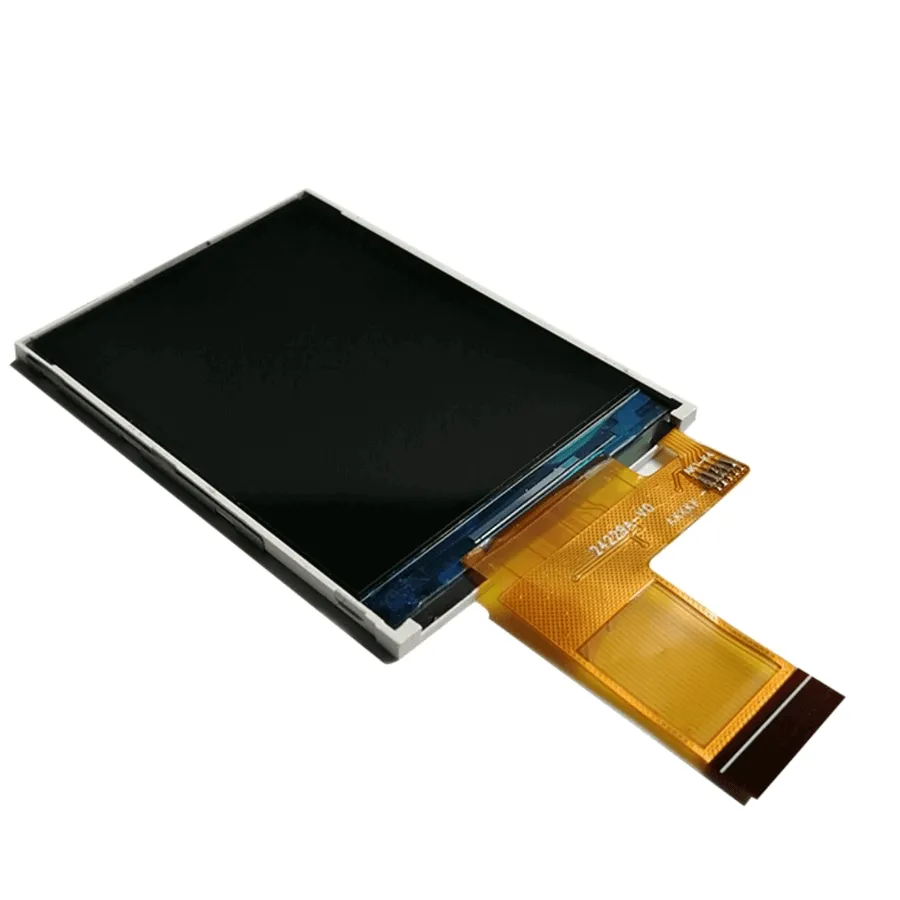
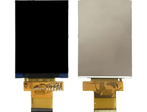
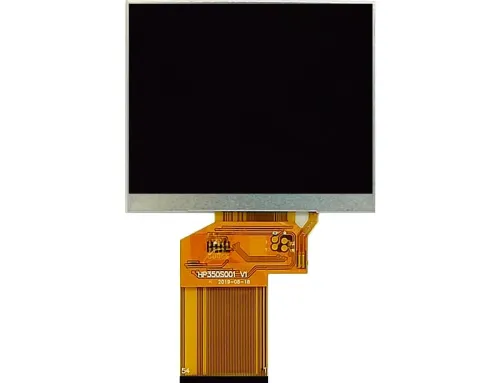
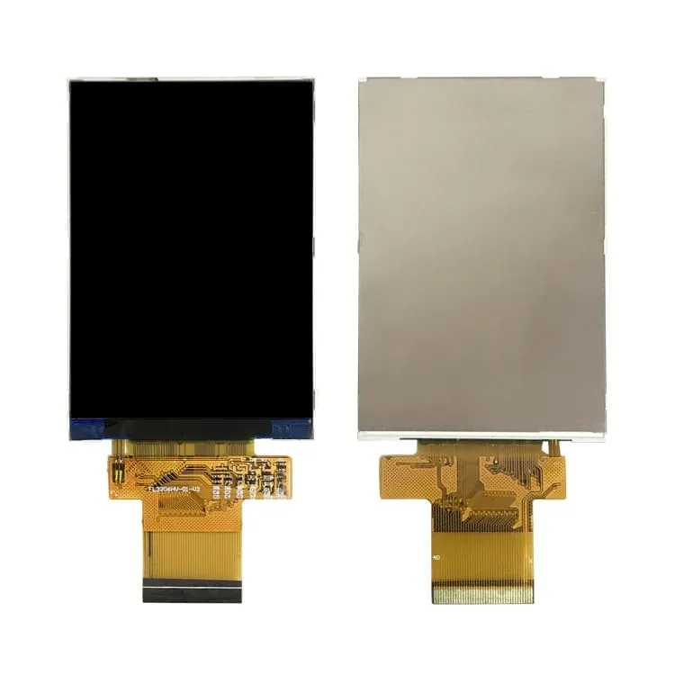
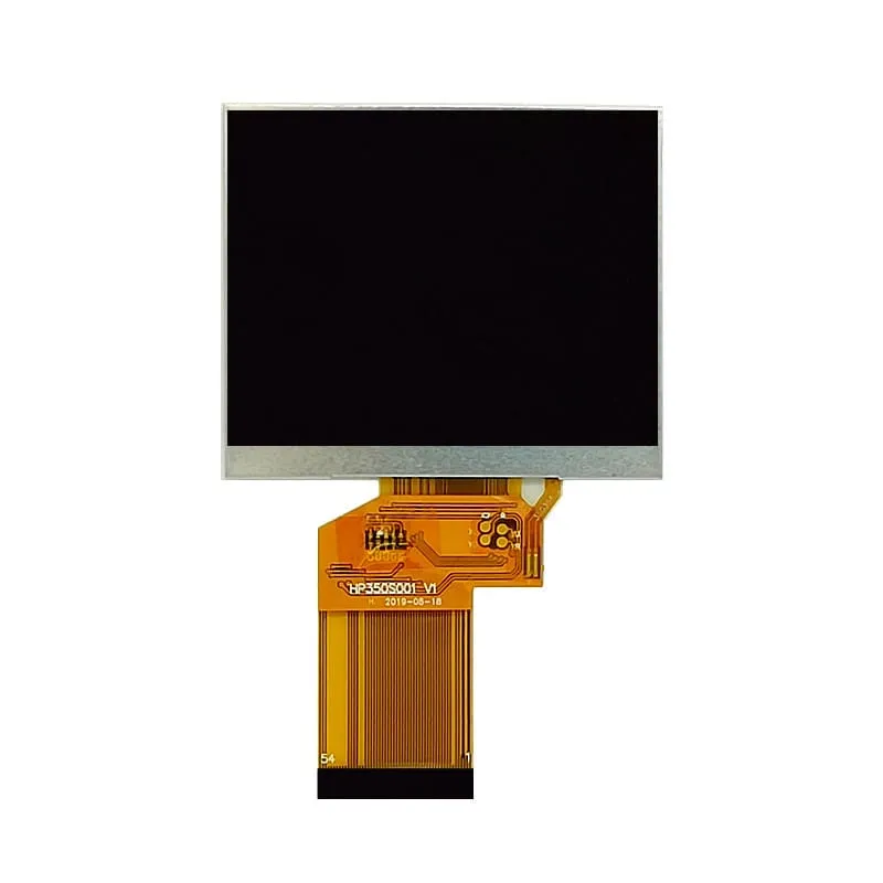
VIS024TN01 is a 2.4″ TFT LCD display module model that adopts TN type LCD with 240*320 resolution. CTP (Capacity Touch Panel) or RTP(Resistive Touch Panel) can be added according to user requirements.
The 2.4-inch TFT-LCD is probably the most sold LCD panel size in the world in terms of unit shipments. It has a wide range of applications and life cycle.
Based on the substantial and long-term shipments of 2.4 inch TFT LCD panels, we can guarantee a stable supply of this LCD display module throughout the life cycle of your product.
Based on the 2.4 inch LCD’s high stability, low price, and excellent storage and operating temperature range, this type of LCD display module can be widely used in feature phones, smart homes, pos machines, industrial instruments (meters), and small medical equipment and other products.
FPCA shape alignment, polarizer material, and backlight brightness can be adjusted according to your needs.
We also supply 2.4″ LCD module(with connector) for NOKIA feature phone repair, models include NOKIA210, NOKIA220, NOKIA3310, NOKIA8810, etc.
Other 2.4 inch TFT LCD display module (LCM) models that can be replaced by VIS024TN01 are COM24H2P29XLC, COM24H2P39ULC, TM024HDH49, etc.
| Panel From | Century/Innolux |
|---|---|
| Panel Size | 2.4 inch |
| Panel Model | CT024TN01 V.X |
| LCM Model | VIS024TN01 |
| Panel Type | a-Si TN TFT-LCD, LCM module |
| Resolution | 240(H) X 320(V) |
| Luminance | 250 cd/m² (Typ.) |
| Display Area | 36.72(H)*48.96(V)(mm) |
| Outline | 42.72(H)*60.26(V)*2.25(T)(mm) |
| Interface Type | 24 pins MCU/SPI |
| View Direction | 12 o’clock |
| Touchscreen | Optional |
| Operating Temperature | -20 ~ 70 °C |
| Storage Temperature | -30 ~ 80 °C |
| Item | Contents | Unit |
| LCM outline dimension | 42.72(W) *60.26(H) * 2.25(T) | mm |
| Module size | 2.4 | inch |
| Resolution | 240(RGB) *320Pixels | – |
| Active area | 36.72(W)*48.96(H) | mm |
| Pixel pitch | – | mm |
| LCD type | TN | – |
| Viewing direction | 12 O’clock | – |
| LCM driver IC | ST7789V | – |
| Backlight type | LEDx4 | – |
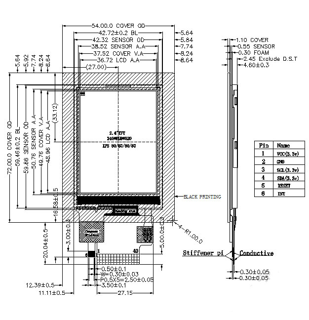
2. STRUCTURAL DRAWING 
| PIN No. | SYMBOL | FUNCTION DESCRIPTION |
|---|---|---|
| 1 | VCC | Power supply for liquid crystal power supply analog circuit. (2.5V-3.3V) |
| 2 | LED _K | Backlight negative |
| 3 | LED _A | Backlight positive |
| 4 | RESET | Reset pin. Setting either pin low initializes the LSI. |
| 5 | CS | Chip select input pin |
| 6 | RS | -Display data/command selection pin in parallel interface. -This pin is used to be serial interface clock. |
| 7 | WR | This pin is used as the serial interface clock in 3wire 9bit/ 4wire 8bit serial data interface. |
| 8 | RD | Read strobe signal in 80-system bus interface operation and enables read operation When RD is low. |
| 9~24 | DB0-DB15 | DATA BUS |
4. ABSOLUTE MAXIMUM RATINGS
| Item | Symbol | MIN | TYP | MAX | Unit |
| Operation Temperature | TOP | -20 | – | 70 | ℃ |
| Storage Temperature | TST | -30 | – | 80 | ℃ |
5.ELECTRICAL CHARACTERISTICS
| Item | Symbol | MIN | TYP | MAX | Unit |
| Logic operating voltage | IOVCC | 1.65 | 1.8 | 3.3 | V |
| Analog operating voltage | VCC | 2.4 | 2.8 | 3.3 | V |
| Input voltage ‘H’ level | VIH | 0.7IOVCC | – | IOVCC | V |
| Input voltage ‘L’ level | VIL | 0 | – | 0.3IOVCC | V |
| Output voltage ‘H’ level | VOH | 0.8IOVCC | – | – | V |
| Output voltage ‘L’ level | VOL | 0 | – | 0.2IOVCC | V |
6.BACKLIGHT CHARACTERISTICS
| Item | Symbol | Typ | Unit |
| Working current | IBL | 4*20=80 | mA |
| Working voltage | VBL | 3.2 | V |
| LCD brightness | L | 250 | CD/M2 |
| X coordinate | 0.27 | 0.29 | 0.31 |
| Y coordinate | 0.27 | 0.29 | 0.31 |
7. OPTICAL CHARACTERISTICS
| Color gamut | S(%) | 60 | % | |||||
| Color chromaticity (CIE1931) | White | Wx | 0.298 | 0.318 | 0.338 | (1)(4) CF glass (C-light) | ||
| Wy | 0.317 | 0.337 | 0.357 | |||||
| Red | Rx | 0.606 | 0.626 | 0.646 | ||||
| Ry | 0.314 | 0.334 | 0.354 | |||||
| Green | Gx | 0.299 | 0.319 | 0.339 | ||||
| Gy | 0.537 | 0.557 | 0.577 | |||||
| Blue | Bx | 0.122 | 0.142 | 0.162 | ||||
| By | 0.102 | 0.122 | 0.142 | |||||
| Viewing angle | Hor. | Left | CR>10 | 35 | 45 | — | ||
| Right | 35 | 45 | — | |||||
| Ver. | Bottom | 35 | 45 | — | ||||
| Top | 10 | 20 | — | |||||
| View Direction | 12 0’clock | (5) | ||||||
| NO. | Test Item | Test Condition | Inspection after test |
| 1 | High-Temperature Storage | 80℃±2℃/120 hours | Inspection after 2~4 hours storage at room temperature, the sample shall be free from below defects: Below defects are not allowed. 1.Air bubble in the LCD 2.Seal leak 3.Non-display 4.Glass crack 5.Current IDD is twice higher than initial value. |
| 2 | Low-Temperature Storage | -30℃±2℃/120 hours | |
| 3 | High-Temperature Operating | 70℃±2℃/120 hours | |
| 4 | Low-Temperature Operating | -20℃±2℃/120 hours | |
| 5 | Temperature Cycle | -20℃±2℃(30min.) ~25℃(5min.) ~70℃±2℃(30min.) 10 cycles | |
| 6 | ESD Test (Non-operating) | Terminals: ±300 V, Contact Panel: ±6 KV, Air | Sample function is normal. |

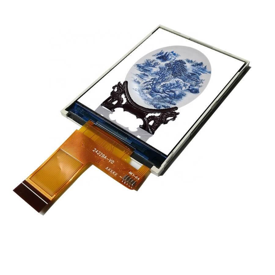
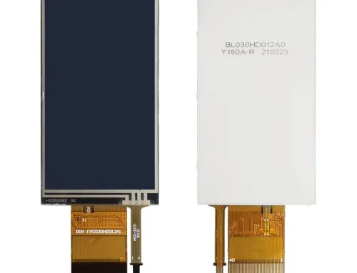
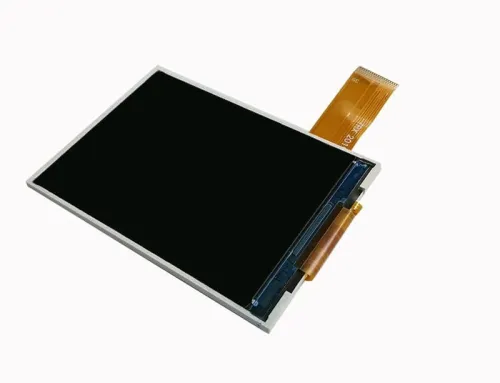
VIS024IPS01 is a 2.4″ TFT display module model that adopts IPS type LCD with 240*320 resolution. CTP (Capacity Touch Panel) or RTP(Resistive Touch Panel) can be added according to user requirements.
This type of LCD display module can be widely used in smart homes, pos machines, industrial instruments (meters), small medical equipment and other products.
FPCA shape alignment, backlight brightness, and touch can all be customized.
| Panel From | BOE/Hannstar |
|---|---|
| Panel Size | 2.4 inch |
| Panel Model | GV024QVQ-N80/HSD024B3N7-A00 |
| LCM Model | VIS024IPS01 |
| Panel Type | a-Si IPS TFT-LCD, LCM module |
| Resolution | 240(H) X 320(V) |
| Luminance | 300 cd/m² (Typ.) |
| Display Area | 36.72(H)*48.96(V)(mm) |
| Outline | 42.72(H)*60.26(V)*2.25(T)(mm) |
| Interface Type | 30 pins RGB/SPI |
| View Direction | ALL |
| Touchscreen | Optional |
| Operating Temperature | -20 ~ 70 °C |
| Storage Temperature | -30 ~ 80 °C |
1. Drawing

2. Pin assignment
|
1 |
GND |
Ground |
|
2 |
VCI |
Power supply for liquid crystal power supply analog circuit. (2.5V-3.3V) |
|
3 |
RESET |
Reset pin. Setting either pin low initializes the LSI. |
|
4 |
CS |
Chip select input pin |
|
5 |
DC(SPI-SCL) |
-Display data/command selection pin in parallel interface. -This pin is used to be a serial interface clock. |
|
6 |
WR(SPI-RS) |
-Write Enable in MCU Parallel Interface. -In 4-fine SPI, this pin is used as D/CX (data/ command selection). -If not used, please fix this pin at VDDI or DGND level. |
|
7 |
VSYNC |
-Vertical (Frame) synchronizing input signal for RGB interface operation. -If not used, please fix the VDDI or DGND. |
|
8 |
HSYNC |
-Horizontal (Line) synchronizing input signal for RGB interface operation. -11001 used, please fix to VDDI or DGND. |
|
9 |
ENABLE |
-Data enable signals for RGB interface operation. -If not used, please fix this pin at VDDI or DGND. |
|
10 |
DOTCLK |
-Display data/command selection pin in parallel interface.–This the pin is used to be a serial interface clock. |
|
11 |
SDA |
The data is applied to the rising edge of the SCL signal. -If not used. fix this pin at VDDI or VSS. |
|
12-16 |
B0-B5 |
GRB data transfer |
|
17-22 |
G0-G5 |
GRB data transfer |
|
23-27 |
R0-R4 |
GRB data transfer |
|
28 |
LED_A |
Backlight positive |
|
29 |
LED_K |
Backlight negative |
|
30 |
GND |
Ground |
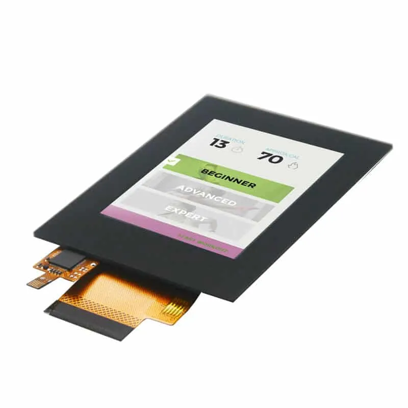
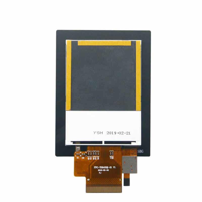

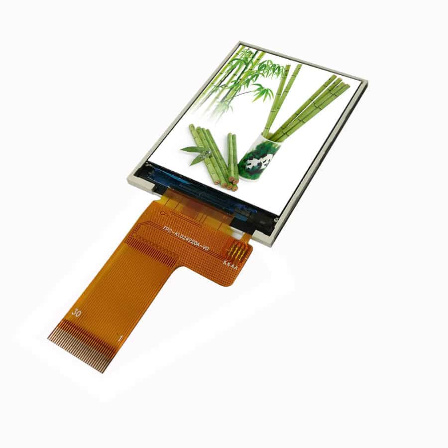
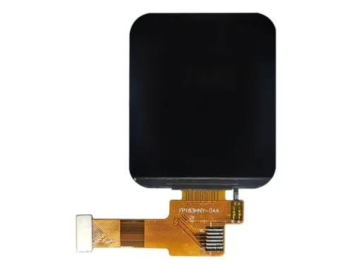
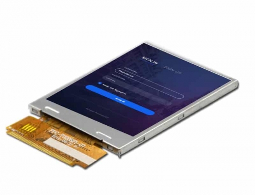
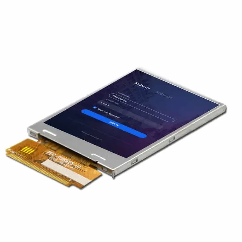
VIS024IPS02C is a 2.4″ TFT display module model that adopts IPS type touch LCD with 240*320 resolution.
This type of LCD display module can be widely used in smart homes, pos machines, industrial instruments (meters), and small medical equipment and other products.
FPCA shape alignment, backlight brightness, and touch can all be customized
| Panel From | BOE/Hannstar |
|---|---|
| Panel Size | 2.4 inch |
| Panel Model | GV024QVQ-N80/HSD024B3N7-A00 |
| LCM Model | VIS024IPS02C |
| Panel Type | a-Si IPS TFT-LCD, LCM module |
| Resolution | 240(H) X 320(V) |
| Luminance | 450 cd/m² (Typ.) |
| Display Area | 36.72*48.96 (mm) |
| Outline | 54.00*72.00*4.60 (mm) |
| Interface Type | 40 pins RGB/SPI/MCU |
| View Direction | ALL |
| Touchscreen | With |
| Operating Temperature | -20 ~ 70 °C |
| Storage Temperature | -30 ~ 80 °C |
1. Drawing
2. Pin assignment
|
Pin No. |
Symbol |
I/O |
Function |
|
1 |
NC |
– |
No connection |
|
2 |
IOVCC |
P |
Digital I/O pad power supply |
|
3-20 |
DB17-DB0 |
I |
data bus |
|
21 |
SDA(SDI) |
I |
When IM3=0, serves as a serial in/out signal. (SDA) When IM3=”1”, serves as a serial in the signal. (SDI) The data is applied to the rising edge of the SCL signal. If not used, fix this pin at IOVCC or GND |
|
22 |
DOTCLK |
I |
Data clock signal for RGB interface operation |
|
23 |
DE |
I |
Data enable signal for RGB interface operation |
|
24 |
HSYNC |
I |
Line sync signal |
|
25 |
VSYNC |
I |
Frame sync signal |
|
26 |
RD |
I |
8080I/8080II system: serves as a read signal an MCU read data at the rising edge. |
|
27 |
WR(D/C) |
I |
8080I/8080II system: serves as a write signal an MCU write data at the rising edge. 4-line system: serves as Data or Command select. In serial interface “2-data-lane data” transfers mode, serves as a second data pin |
|
28 |
DC(SCL) |
I |
(DC)This pin is used to select “Data or Command” in the parallel interface SCL:Serial data clock in a serial bus system |
|
29 |
CS |
I |
Chip select signal |
|
30 |
RESET |
I |
System Reset |
|
31-34 |
IM0-IM3 |
I |
System interface select. |
|
35 |
NC |
– |
No connection |
|
36 |
GND |
P |
Ground. |
|
37 |
VCI |
P |
Power supply |
|
38 |
NC |
P |
No connection |
|
39 |
LED-A |
P |
LED backlight(Anode) |
|
40 |
LED-K |
P |
LED backlight(Cathode) |